The world of computing and electronics has undergone a massive transformation since the invention of semiconductor transistors, and eventually Very Large Scale Integration (VLSI). The idea of integrating millions or even billions of these transistors into a single microprocessor chip opened a new world of possibilities, especially for new professionals delving into this field.
These minute marvels are the brains behind any smart device today, from simple smartphones to advanced supercomputers. However, the process of creating a working physical chip is complex and meticulous, and it’s what is called the physical design flow in VLSI.
In our definitive guide, we will delve into exploring the intricacies of VLSI physical design flow, analysing each step to help you understand how a microchip is built. Whether you’re an upcoming VLSI engineer or just curious about the process of making a chip, this guide will reveal the process for you.
What is Physical Design in VLSI?
You’ve probably come across the concept of physical design severally when researching VLSI technology. Well, the process is all about how the logical form of an Integrated Circuit (IC) is transformed into a physical design layout which is then fabricated using silicon. It’s a complex procedure that involves transforming high-level design descriptions into a netlist, which is then mapped onto a silicon substrate.
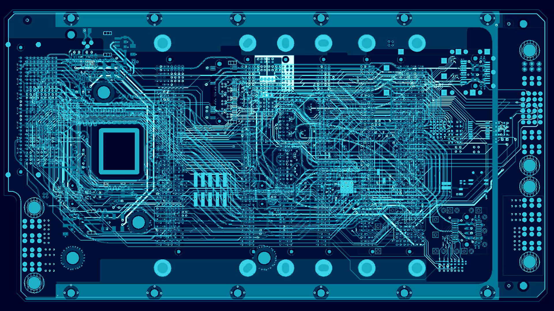
The outcome is a comprehensive physical design of the microchip, complete with how transistors are positioned, routed, and interconnected. The VLSI design flow entails a myriad of compounded steps aimed at creating a chip that meets performance, power, and other requirements. While the chip has to be within the required standards, it must also adhere to the limitations of manufacturing.
Why is the Design Flow in VLSI Important?
VLSI design flow has a crucial significance in the process of building a microprocessor chip. Firstly, it offers a systematic guideline and structured process to ensure consistency and replicability in chip manufacturing. Chip designers, through the design flow, minimize the possibility of errors or inconsistencies, which is crucial in creating highly efficient and reliable ICs.
The process of making a chip involves different teams coordinating together to achieve a common goal. Therefore, it’s crucial to have a unified form of communication and collaboration, and that is where the VLSI design flow comes in. The PD flow in VLSI standardises the process, allowing engineers to easily comprehend their colleague’s work. This makes it easier to spot and rectify errors or other issues arising from the design process.
More importantly, the physical design flow in VLSI is important in design optimization for different parameters such as timing, performance, power consumption, and area. As the process flows through the various phases, engineers are empowered through informed decisions to attain the required balance between the parameters. Through optimization, the engineers can ensure that the product adheres to specifications and performs optimally in a real-world scenario.
The Stages of Physical Design Flow in VLSI
In practice, VLSI kicks off at the point where the physical design flow ends. Due to the complexity of physical design flow in VLSI, the steps are subdivided into different main processes. Let’s take a look at the key phases of the PD flow in VLSI.
1. Specification and High-Level Design
The process kicks off with the definition of the desired performance and functionality features of the microchip. The high-level design comes next and involves building the chip’s top-level architectural representation. The latter outlines the major components of the chip and their roles. At this phase, VLSI flow charts and block diagrams are used commonly for representation.
2. Register Transfer Level (RTL) Design and Simulation
At the RTL design phase, the logical description of the microprocessor’s behaviour is built using hardware description languages such as Verilog or VHDL. During this stage, the engineers design the modules, define the interfaces, and simulate the chip’s functionality to confirm that it conforms to the specifications. RTL simulation is also crucial in identifying and correcting any logical errors that may arise.
3. Synthesis
During the synthesis phase, the code from the RTL stage undergoes synthesis to form a gate-level representation. The synthesis phase entails mapping the logical functions to standard cell libraries, which are then optimised for power, area, and timing.
The product of this process is a gate-level netlist defining the structure of the chip but not the physical layout.
4. Floor Planning
The floor planning stage is another complex phase of the process. It entails space allocation on the silicon substrate for various functional blocks. This being a crucial phase, the engineers must consider key factors such as signal routing, thermal constraints, and power distribution. The primary goal of this stage is to attain an efficiently balanced microchip layout.
5. Placement
During the placement stage, engineers determine the exact position of every standard cell in the allotted area of the chip. This is achieved using an advanced placement tool with pre-defined algorithms that minimise the wire length while optimizing for power, timing, and area. These tools utilise global and detailed placement stages for optimal results.
Placement does not only place the standard cells in the netlist, but it also positions several other physical cells while adding buffers as per the specifications to achieve the timings.
6. Clock Tree Synthesis (CTS)
CTS is an important stage of the physical design flow in VLSI which ensures the clock signals are uniformly distributed to every sequential element in the design. This in turn minimises skew and jitter. It simply involves inserting the buffers along the design’s clock paths to attain minimum skew.
Clock Tree Synthesis aims to achieve the constraints of the clock tree design rule such as maximum load capacitance, maximum transition, and maximum fanout. All these constraints must be met for the insertion delay and skew to be minimised.
7. Routing
Routing is responsible for connecting the cells to the block. During the routing phase, all components on the chip including the standard cells get connected as per the placement results and synthesised netlist. The process entails routing wires while optimizing for specifications such as congestion and timing.
Routing can be global, track assignment, detailed, or search and repair. Global routing is used for assigning routing resources and keeping track of the assignments in a network. On the other hand, detailed routing is responsible for making actual connections and repairing Design Rule Checks (DRC) violations.
8. Physical verification
Before progressing to fabrication, designers perform verification checks to ensure that the layout meets the manufacturing constraints and rules. The process includes DRC, electrical rule checking (ERC), and layout vs. schematic (LVS) verification. An equivalence check is also done during this phase and it compares the built netlist to the one generated by the tool.
Design Rule Check is done to verify if the provided layout meets the design rules from the fabrication team.
9. Extraction and Timing Analysis
At this phase of the physical design flow in VLSI, a parasitic extraction is done to assess the performance of the chip. The process closely monitors and accounts for the effects produced by the resistance and capacitance on signal propagation.
Timing analysis is performed to ascertain if the microchip adheres to its performance objectives.
10. Final Sign-off and Tapeout
After passing all the checks and it’s confirmed that the design conforms to the specifications, it’s ready for Tapeout. This simply means preparing the design data into a format that meets semiconductor fabrication requirements. Once all is done, the chip is ready for manufacturing.
At the foundry, advanced manufacturing procedures are used in building the physical integrated circuit according to the layout specifications. Some of the processes include photolithography, deposition, and etching. After Tapeout, the post-tapeout activities such as package design, testing, and debugging may follow to ensure the microchip works as intended.
Challenges of The Physical Design Flow in VLSI
The physical design flow in VLSI solves the complexities that would otherwise be impossible to tackle when building a chip. Despite all the benefits, VLSI design flow also comes with its shortcomings that engineers have to tackle. Some of these include:
Design complexity
As the number of transistors integrated into a chip increases, so does the chip’s complexity. As such, the PD flow in VLSI also grows intricacy, making it more challenging for teams to work with them. Therefore, advanced tools and methodologies have to be created for the successful implementation of a design flow.
Technology scaling
With every semiconductor technology advancement, comes the need for design flows to advance to conform to the new design constraints and processes. For manufacturers to keep up with this technology scaling, they need continuous learning programs in place while updating their design methodologies.
Power management
One of the most critical challenges in VLSI physical design is the efficient management of power consumption. Every design flow must have a power optimisation method that reduces the consumption of power while retaining the desired specifications.
Marketing time constraints
Technological advancements are changing at a rapid pace, which demands reduced marketing time for any VLSI products. Therefore, designers and engineers need to optimise the PD flow in VLSI to reduce the time consumed at each stage without compromising the product’s quality.
Conclusion
The physical design flow in VLSI is an intricate and multi-disciplinary process involving computer science, electrical engineering, and material science. All these disciplines function interdependently to build powerful microchips that power the world of computing. Right from conception to completion, each phase has a significant contribution in providing the chip with the desired performance, functionality, and reliability.
This definitive guide provides crucial information and an overview of physical design flow while highlighting some of the complexities involved at each stage. While the guide provides a comprehensive understanding, it’s worth noting that VLSI design flow is a complex discipline that is continuously evolving. New techniques and tools are emerging regularly making it more challenging to master the VLSI concept. However, undertaking a VLSI physical design course gives you a more comprehensive understanding of VLSI physical design and prepares you for a professional career take-off. Kickstart your journey to becoming a qualified VLSI engineer with a professional course from Aiit Institute today.

